SOLO-PV Solution-based Low-cost PhotoVoltaics
In the SOLO-PV project we developed low-cost fabrication processes and materials for thin film photovoltaics (TFPV) of the 3rd generation. The project focused on the copper-zinc-tin-sulfur-selenium (CZTSSe) absorber – a compound semiconductor, which contains only earth abundant elements and can lead to high power conversion efficiencies, similar to other commercial TFPV technologies. The CZTSSe absorber was deposited by solution-based methods, namely chemical spray pyrolysis (CSP), electrochemical deposition (ECD) and spin coating, followed by a thermal treatment to induce the desired kesterite crystal phase. Along with the absorber, SOLO-PV used chemical bath deposition (CBD) to deposit cadmium-free buffer layers of ZnS and InSx, as well as ECD and CSP for the ZnO window layer and the doped ZnO transparent contact. SOLO-PV has therefore evaluated a range of solution-based techniques and materials that bear the potential to drastically reduce the cost of TFPV and foster their deployment and their integration into the built environment.
Ausgangssituation
The photovoltaics (PV) market is currently dominated (>80%) by the crystalline silicon (c-Si) technology. The rest of the market is covered by TFPV, which however has a high potential to increase its share in the near future. Indeed, TFPV can be produced with lower material consumption and by high throughput processes, thus enabling a marked price reduction per Watt-peak. Besides, thin film modules can be also deposited on flexible substrates (e.g. plastic or steel foils), making their integration easier in the built-environment and in applications where light weight and flexibility are prioritized. Today, the main commercial thin film technologies are based on the cadmium telluride (CdTe) and the copper-indium-gallium-sulfur(selenium) (CIGSSe) absorbers. While these absorbers offer similar high efficiencies to c-Si, they contain toxic (like Cd) or rare elements (like In). This drives the research for other efficient technologies based on abundant and non-toxic absorbers such as the CZTSSe. This drive is not limited to the absorber itself but concerns all material components of the solar cell (transparent electrode, buffer and window layer) along with their fabrication processes.
The International Energy Agency PV Technology Roadmap summarized the main industry manufacturing aspects and R&D areas for the current and possible up-coming PV thin film technologies until 2030. Any new successful TFPV concept should address as many as possible of these issues in order to be able to compete with the current main players of CIGS and CdTe. SOLO-PV was the first stage of a project chain, which aims to address the following manufacturing and R&D aspects, as identified by the IEA.
Manufacturing aspects: Simplified production processes; Management of toxic materials; Improved deposition techniques; Large, high-efficiency production units; Availability of manufacturing materials; Improved cell structures; Improved deposition techniques; Advanced materials and concepts
R&D aspects: Improved cell structures; Improved deposition techniques; Advanced materials and concepts
Projektverlauf
The project was constructed in 5 workpackages (WP). WP1 concerned the developement of the CZTSSe absorber, WP2 of the buffer, WP3 of the transparent contact. WP4 tackled the integration of all materials into solar cells and their PV characterization and evaluation. Finally, project management and dissemination tasks were intgrated in WP5.
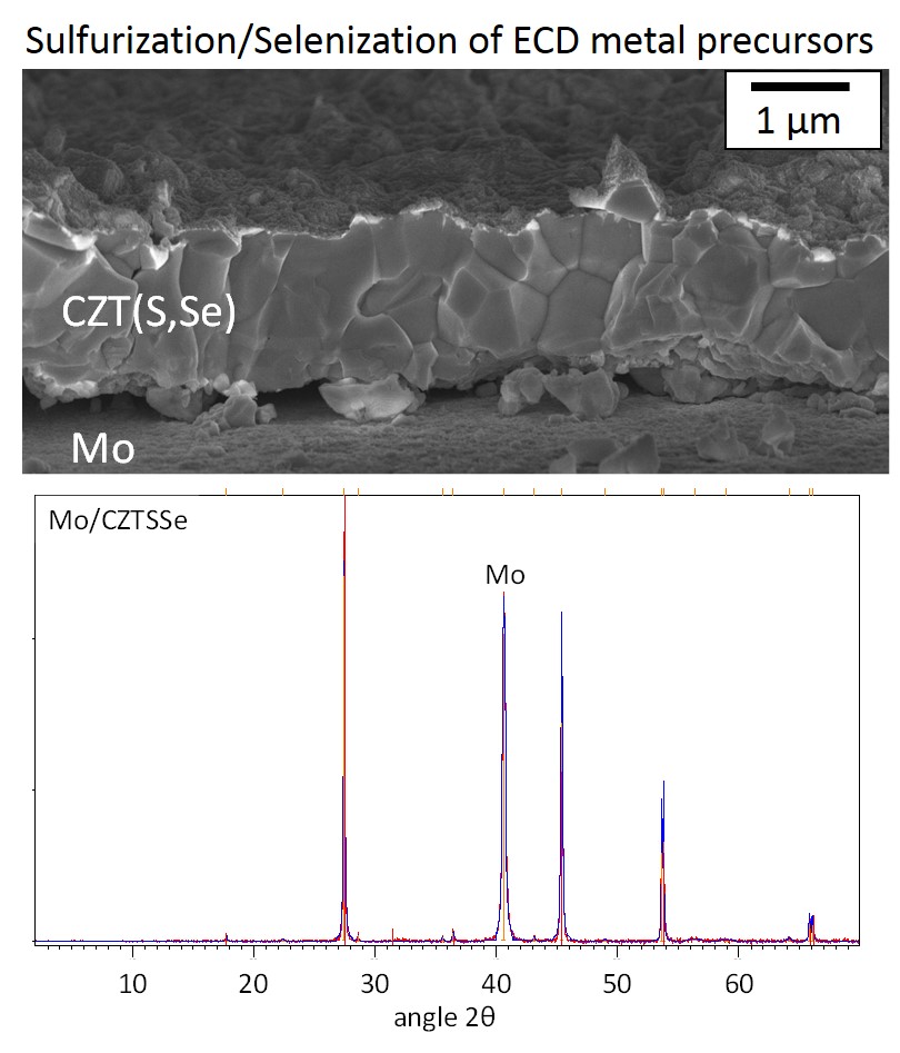
The experimental tasks in the project began with the development of the kesterite absorber using different solution-based techniques. EMPA concentrated on CSP and spin-coating, while AIT on ECD. A two-step approach for the absorber formation was followed in all cases: firstly a precursor (multi)layer was deposited on the molybdenum-coated substrate, which was then transformed into the kesterite phase by thermal sulfurization/selenization. The deposition was optimized in the course of more than 2 years. The optimized films had the appropriate composition, kesterite crystal structure and energy bandgap. However, the presence of certain secondary phases could not be excluded and in certain cases films presented a pronounced porosity.
In parallel to the absorber development, efforts were invested in replacing the CdS buffer layer with Cd-free alternatives based on ZnS (fabricated by CSP at EMPA) and InSx (fabricated by CBD at AIT). CSP-ZnS films processed at higher temperatures (350 °C) showed some texture, but the lower temperature processed films of ZnS, as well as the InSx were amorphous/nanocrystalline. All buffers had the expected bandgap values.
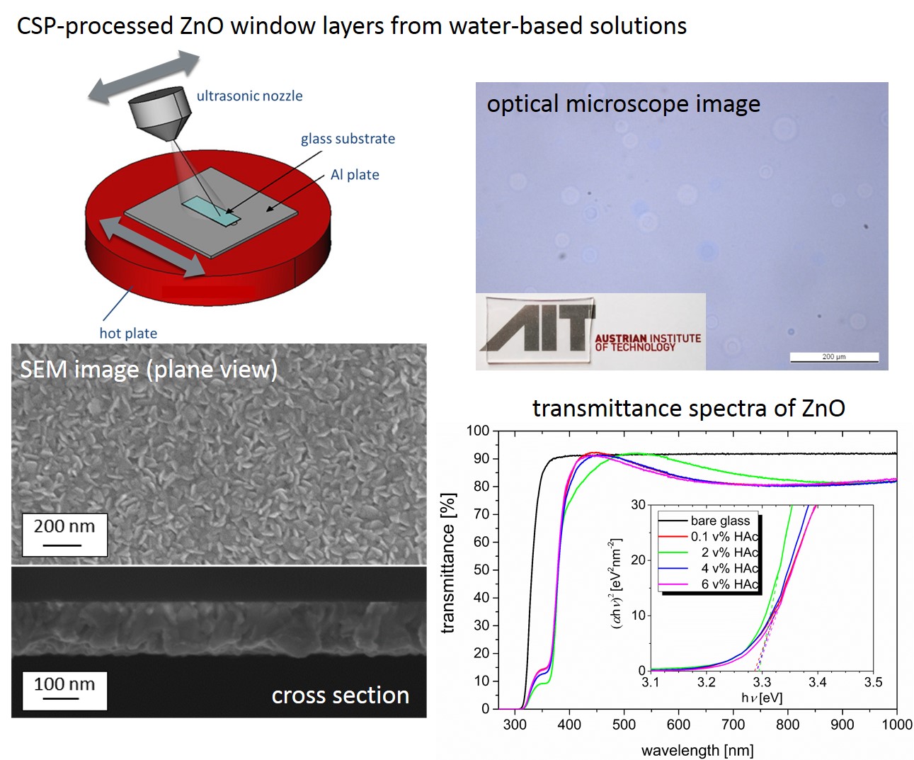
At the same time, EVG and AIT have intensified their cooperation for the development of a ZnO-based window layer and transparent conductive oxide by CSP. The target was to develop chemical solutions for spraying that were explicitly water-based (no organic solvents like alcohols), in order to facilitate the processing at the required high substrate temperatures. At the same time, we tried to keep the deposition temperature below 400 °C and use only low-cost and abundant chemical reagents. The resulting ZnO films were, indeed, highly crystalline, compact and transparent. Complementary to that, AIT processed doped ZnO films by ECD, using again water-based solutions and temperatures below 90 °C.
In WP4 the aforementioned layers and process were integrated into solar cell devices that were evaluated in terms of photovoltaic performance. Cells incorporating the kesterite absorber processed by spin-coating and subsequent thermal selenization presented the highest power conversion efficiency, which exceeded 8%, while CSP-processed kesterite cells yielded efficiency lower than 1% and ECD-processed cells suffered from micro-shunts.
Meilensteine
- Established chemical spray pyrolysis of CZTS on Zn/metal and/or glass substrate
- Established electrochemical deposition of CZTS on Zn/metal and/or glass substrate
- Established chemical spray pyrolysis of ZnS on CZTS
- Established electrochemical deposition of ZnS on CZTS
- Established chemical spray pyrolysis of TCO on buffer layer
- Established electrochemical deposition of TCO on buffer layer
- First electrical and optical characterization of finished solar cell devices
- : Decisive point on superior solar cell materials and related fabrication sequence
- Electrical and optical characterization of optimized solar cell devices
Ergebnisse
The main results of the project can be summarized as follows:
a) We demonstrated CZTS(Se) absorber layer sprayed in a sequence of Cu-, followed by Zn-, Sn- and sulfur-containing alcoholic solutions. Sequential spraying provided a greater flexibility in terms of molarity and reduced the possibility of instable solutions. The effect of different sulfur source on the Zn/Sn metal ratio was investigated and a reduction of Zn loss was found when using thioacetamide. Reducing the Sn concentration led to the desired Zn-rich film formation.
b) CZTSe absorber with state-of-the-art properties was developed by spin-coating metal salts dissolved in DMSO solution and subsequent selenization. The effect of sodium content in improving the CZTSe properties was demonstrated.
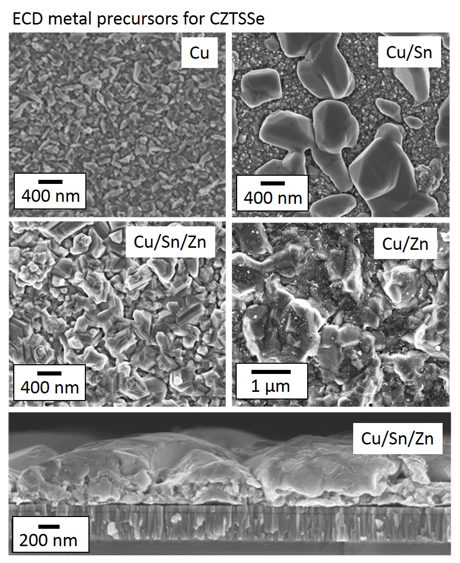
c) We demonstrated that high quality metallic precursor layers for CZTS(Se) can be deposited electrochemically, using mild aqueous solutions and low temperatures. The stoichiometry of the metals in the final kesterite absorber can be tuned by adjusting their respective layer thickness. Kesterite films could be obtained after the chalcogenization process.
d) Buffer layers of ZnS and InSx with appropriate properties were developed by chemical spray pyrolysis and chemical bath deposition, respectively, as alternatives to the standard CdS buffer used in kesterite cells.
e) Transparent and conductive ZnO and aluminum-doped ZnO (AZO) layers were developed using electrochemical deposition, from aqueous solutions and temperatures below 90oC.
f) ZnO, and aluminum-doped ZnO layers were developed by the spray pyrolysis technique from exclusively water-based solutions, at temperatures below 400 oC and with high quality structural, optical and electrical properties.
g) CZTSe solar cells formed by spray pyrolysis showed an energy conversion efficiency of 0.7%. CZTSe cells formed by spin coating showed efficiency larger than 8%. ECD-grown kesterite cells suffered from shunts. The work for addressing the shunt issue is currently on-going.
Following conclusions could be drawn:
a) The chemical spray pyrolysis method for CZTS(Se) is feasible but not suitable for producing efficient absorber films. On the contrary, the spin-coating technique is the solution process of choice for efficient CZTS(Se) solar cells.
b) The sequential potentiostatic electrodeposition of metallic thin film precursors is a very promising technique for kesterite CZTS(Se) absorber, since it is upscalable, uncomplicated in terms of solution preparation, we can easily adjust the composition through the thickness of the metallic constituents and the deposition takes place close to room temperature.
c) Alternative buffer layers of ZnS and In2S3 are not yet capable to replace CdS in producing efficient CZTS(Se) cells.
d) It is possible to produce intrinsic and doped-ZnO layers by CSP using exclusively water-based solutions, with layer properties similar to solutions with alcohol-content. Water-based solutions greatly facilitate the processing, as the high temperatures used for spray pyrolysis demand strict safety measures when an alcohol-containing solvent is employed.
e) Compact and highly transparent ZnO and doped-ZnO layers can be fabricated by ECD.
f) It is possible to prepare a complete solar cell using exclusively low-cost, solution-based processing for all components, i.e. transparent contact, absorber, buffer.
Peer-reviewed publications
[1] S. Abermann, Non-vacuum processed next generation thin film photovoltaics: Towards marketable efficiency and production of CZTS based solar cells, Sol. Energy. 94 (2013) 37–70. doi:10.1016/j.solener.2013.04.017.
[2] S. Edinger, J. Bekacz, M. Richter, R. Hamid, R.A. Wibowo, A. Peić, T. Dimopoulos, Influence of the acetic acid concentration on the growth of zinc oxide thin films prepared by spray pyrolysis of aqueous solutions, Thin Solid Films. (2015). doi:10.1016/j.tsf.2015.04.027.
[3] R.A. Wibowo, R. Hamid, T. Maier, T. Dimopoulos, Galvanostatically-electrodeposited Cu–Zn–Sn multilayers as precursors for crystallising kesterite Cu2ZnSnS4 thin films, Thin Solid Films. 582 (2015) 239–244. doi:10.1016/j.tsf.2014.10.060.
[4] M. Werner, C.M. Sutter-Fella, H. Hagendorfer, Y.E. Romanyuk, A.N. Tiwari, Cu2ZnSn(S,Se)4 solar cell absorbers processed from Na-containing solutions in DMSO: Cu2ZnSn(S,Se)4 solar cell absorbers, Phys. Status Solidi A. 212 (2015) 116–120. doi:10.1002/pssa.201431146.
Downloads
Steckbrief
-
Projektnummer834655
-
KoordinatorAIT Austrian Institute of Technology GmbH
-
ProjektleitungTheodoros Dimopoulos, theodoros.dimopoulos@ait.ac.at
-
Partner
-
FörderprogrammNeue Energien 2020
-
Dauer01.2012 - 04.2017
-
Budget878.278 €


